S3C2440A Memory Map after Reset
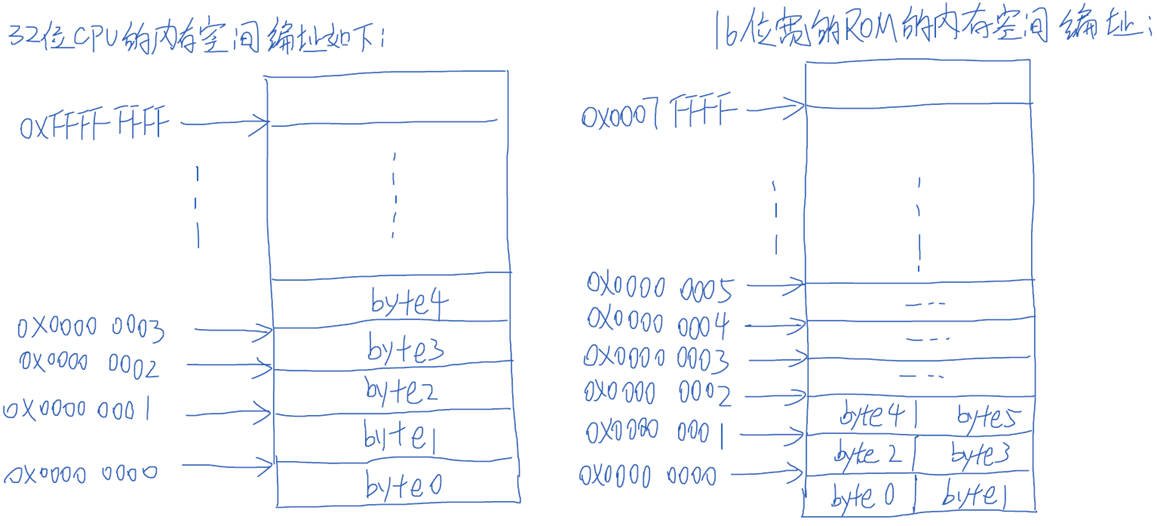
S3C2440的内存空间划分为不同的块,当CPU向内存控制器发出地址,内存控制器根据地址范围,发出对应片选信号到片选引脚,实现对不同设备的控制。
BANK0 BUS WIDTH
The data bus of BANK0 (nGCS0) should be configured with a width as one of 16-bit and 32-bit ones. Because the BANK0 works as the booting ROM bank (map to 0x0000_0000), the bus width of BANK0 should be determined before the first ROM access, which will depend on the logic level of OM[1:0] at Reset.

MEMORY (SROM/SDRAM) ADDRESS PIN CONNECTIONS

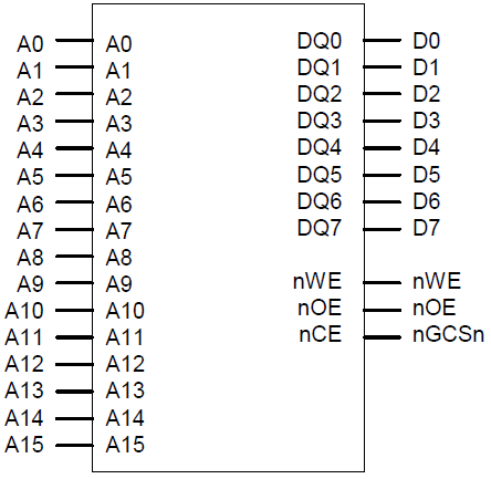
Memory Interface with 8-bit ROM
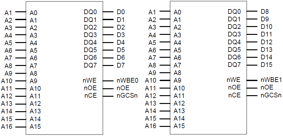
Memory Interface with 8-bit ROM x 2
Memory Interface with 8-bit ROM x 4

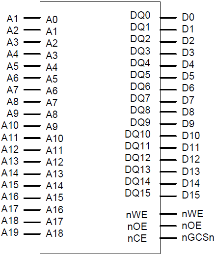
Memory Interface with 16-bit ROM
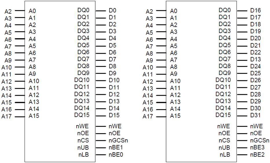
Memory Interface with 16-bit SRAM x 2
分析:
以《Memory Interface with 16-bit ROM》为例:
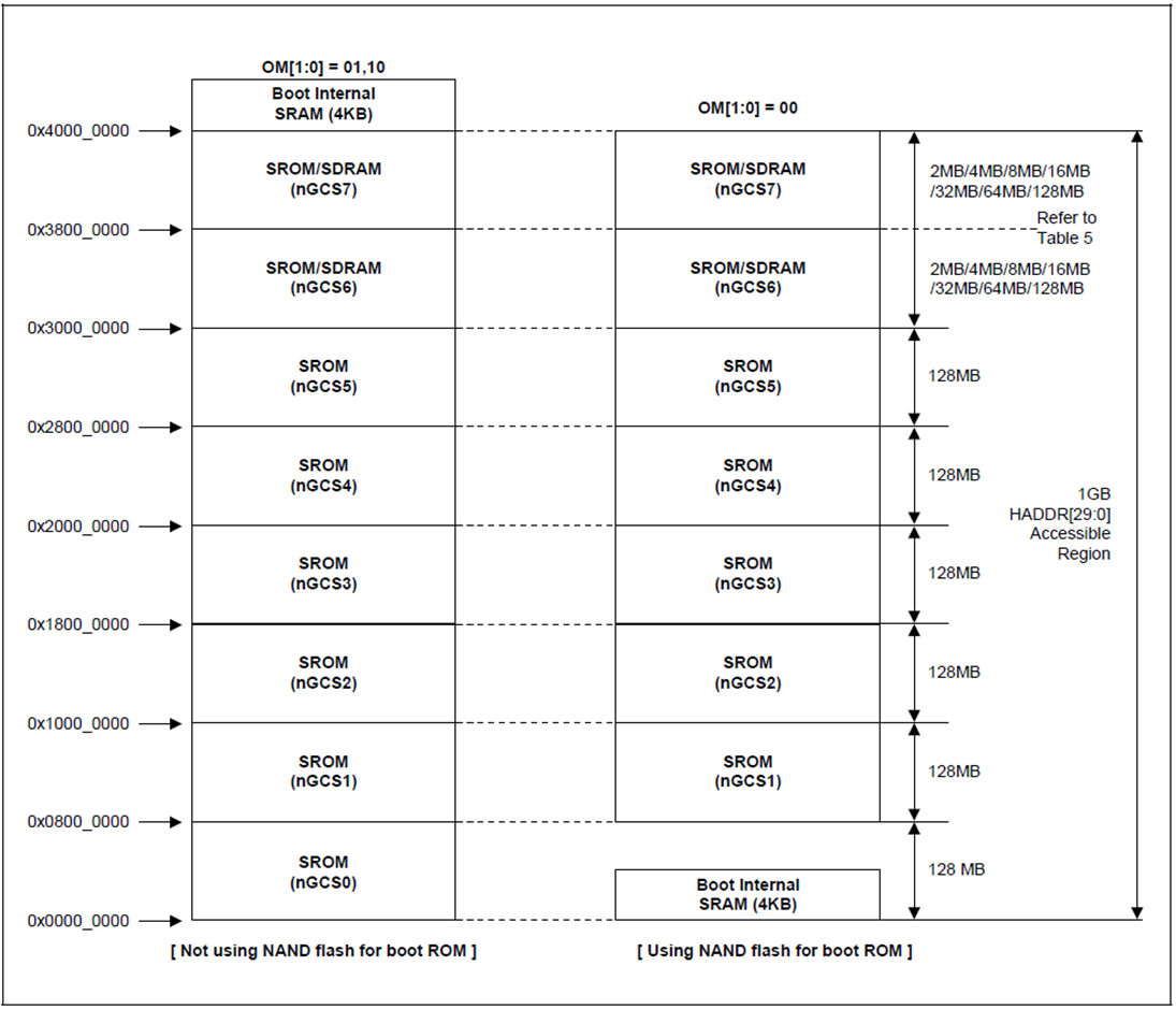
CPU是按字节寻址的;位宽为16的ROM是按半字寻址的(半字等于两个字节);
A0连接CPU的哪根地址线,是由存储芯片的数据位宽决定的。由于这个ROM是按半字寻址的,所以CPU访问这个ROM时应该进行地址转换。
